- 您现在的位置:买卖IC网 > Sheet目录341 > MAX8702ETP+ (Maxim Integrated Products)IC DRVR MOSFET DUAL 20-TQFN
Dual-Phase MOSFET Drivers
with Temperature Sensor
ABSOLUTE MAXIMUM RATINGS
V CC to AGND............................................................-0.3V to +6V
V DD to AGND............................................................-0.3V to +6V
PGND_ to AGND ...................................................-0.3V to +0.3V
SKIP , SHDN , DRHOT , TSET to AGND......................-0.3V to +6V
PWM_ to AGND ........................................................-0.3V to +6V
DL_ to PGND_ ............................................-0.3V to (V DD + 0.3V)
LX_ to AGND .............................................................-2V to +30V
DH_ to LX_ ...............................................-0.3V to (V BST_ + 0.3V)
BST_ to LX_ ..............................................................-0.3V to +6V
Continuous Power Dissipation (T A = +70°C)
20-Pin 4mm x 4mm Thin QFN
(derate 16.9mW/ ° C above +70°C) .............................1349mW
Operating Temperature Range .........................-40°C to +100°C
Junction Temperature ......................................................+150°C
Storage Temperature Range .............................-65°C to +150°C
Lead Temperature (soldering, 10s) .................................+300°C
Stresses beyond those listed under “Absolute Maximum Ratings” may cause permanent damage to the device. These are stress ratings only, and functional
operation of the device at these or any other conditions beyond those indicated in the operational sections of the specifications is not implied. Exposure to
absolute maximum rating conditions for extended periods may affect device reliability.
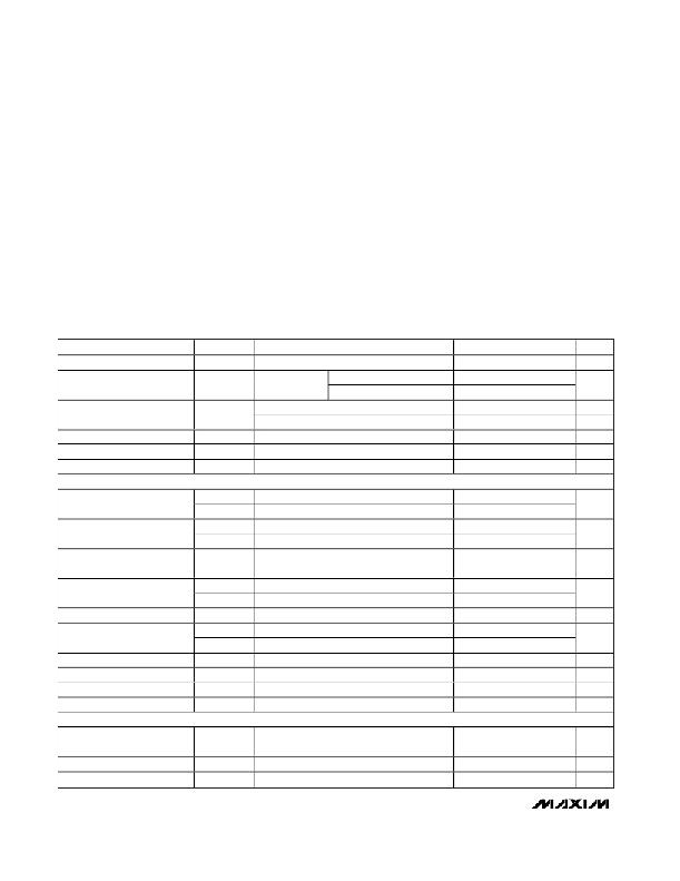
ELECTRICAL CHARACTERISTICS
(Circuit of Figure 2. V CC = V DD = V SHDN = V SKIP = 5V, T A = 0°C to +85°C . Typical values are at T A = +25°C, unless otherwise noted.)
PARAMETER
Input Voltage Range
SYMBOL
V CC
CONDITIONS
MIN
4.5
TYP
MAX
5.5
UNITS
V
V CC Undervoltage-Lockout
Threshold
V UVLO
85mV typical
hysteresis
V CC rising
V CC falling
3.4
3.3
3.85
3.75
4.1
4.0
V
V CC Quiescent Current
(Note 1)
V DD Quiescent Current
V CC Shutdown Current
V DD Shutdown Current
I CC
I DD
SKIP = AGND, PWM_ = AGND
SKIP = AGND, PWM_ = V CC
SKIP = AGND, PWM_ = AGND
SHDN = SKIP = AGND
SHDN = SKIP = AGND
200
2
1
2
1
400
3
5
5
5
μA
mA
μA
μA
μA
GATE DRIVERS AND DEAD-TIME CONTROL (Figure 1)
DL_ Propagation Delay
DH_ Propagation Delay
DL_ Transition Time
DH_ Transition Time
t PWM-DL
t DH-DL
t DL-DH
t PWM-DH
t F _ DL
t R _ DL
t F _ DH
t R _ DH
PWM_ high to DL_ low
DH_ low to DL_ high
DL_ low to DH_ high
PWM_ low to DH_ low
DL_ falling, 3nF load
DL_ rising, 3nF load
DH_ falling, 3nF load
DH_ rising, 3nF load
19
36
25
23
11
8
14
16
ns
ns
ns
ns
DH_ On-Resistance (Note 2)
DL_ On-Resistance (Note 2)
DH_ Source/Sink Current
R DH
R DL _ HIGH
R DL _ LOW
I DH
V BST _ - V LX _ = 5V
High state (pullup)
Low state (pulldown)
V DH _ = 2.5V, V BST _ - V LX _ = 5V
1.0
1.0
0.35
1.5
4.5
4.5
2.0
?
?
A
DL_ Source Current
I DL _ SOURCE V DL _ = 2.5V
1.5
A
DL_ Sink Current
Zero-Crossing Threshold
I DL _ SINK
V DL _ = 5V
V PGND _ - V LX _, SKIP = AGND
5
2.5
A
mV
TEMPERATURE SENSOR
Temperature Threshold
Accuracy
DRHOT Output Low Voltage
DRHOT Leakage Current
T A = +85 ° C to +125 ° C, 10 ° C falling hysteresis
I SINK = 3mA
High state, V DRHOT = 5.5V
-5
+5
0.4
1
° C
V
μA
2
_______________________________________________________________________________________
发布紧急采购,3分钟左右您将得到回复。
相关PDF资料
MAX8790AETP+T
IC LED DRVR WHITE BCKLGT 20-TQFN
MAX8790ETP+T
IC LED DRVR WHITE BCKLGT 20-TQFN
MAX8791GTA+
IC MOSFET DRIVER 8-TQFN
MAX8811EEE+
IC DRVR DL PHASE HS 16-QSOP
MAX8821ETI+
IC LED DRVR WHITE BCKLGT 28-TQFN
MAX8822ETE+T
IC LED DRVR WHITE BCKLGT 16-TQFN
MAX8830EWE+T
IC LED DRVR WHITE BCKLGT 16-UCSP
MAX8831EWE+T
IC LED DRIVR WHITE BCKLGT 16-WLP
相关代理商/技术参数
MAX8702ETP+T
功能描述:功率驱动器IC Dual-Phase MOSFET Driver w/Temp Sensor RoHS:否 制造商:Micrel 产品:MOSFET Gate Drivers 类型:Low Cost High or Low Side MOSFET Driver 上升时间: 下降时间: 电源电压-最大:30 V 电源电压-最小:2.75 V 电源电流: 最大功率耗散: 最大工作温度:+ 85 C 安装风格:SMD/SMT 封装 / 箱体:SOIC-8 封装:Tube
MAX8702ETP-T
功能描述:功率驱动器IC RoHS:否 制造商:Micrel 产品:MOSFET Gate Drivers 类型:Low Cost High or Low Side MOSFET Driver 上升时间: 下降时间: 电源电压-最大:30 V 电源电压-最小:2.75 V 电源电流: 最大功率耗散: 最大工作温度:+ 85 C 安装风格:SMD/SMT 封装 / 箱体:SOIC-8 封装:Tube
MAX8703ETP
功能描述:功率驱动器IC RoHS:否 制造商:Micrel 产品:MOSFET Gate Drivers 类型:Low Cost High or Low Side MOSFET Driver 上升时间: 下降时间: 电源电压-最大:30 V 电源电压-最小:2.75 V 电源电流: 最大功率耗散: 最大工作温度:+ 85 C 安装风格:SMD/SMT 封装 / 箱体:SOIC-8 封装:Tube
MAX8703ETP+T
功能描述:功率驱动器IC RoHS:否 制造商:Micrel 产品:MOSFET Gate Drivers 类型:Low Cost High or Low Side MOSFET Driver 上升时间: 下降时间: 电源电压-最大:30 V 电源电压-最小:2.75 V 电源电流: 最大功率耗散: 最大工作温度:+ 85 C 安装风格:SMD/SMT 封装 / 箱体:SOIC-8 封装:Tube
MAX8703ETP-T
功能描述:功率驱动器IC RoHS:否 制造商:Micrel 产品:MOSFET Gate Drivers 类型:Low Cost High or Low Side MOSFET Driver 上升时间: 下降时间: 电源电压-最大:30 V 电源电压-最小:2.75 V 电源电流: 最大功率耗散: 最大工作温度:+ 85 C 安装风格:SMD/SMT 封装 / 箱体:SOIC-8 封装:Tube
MAX8704EUB
功能描述:低压差稳压器 - LDO RoHS:否 制造商:Texas Instruments 最大输入电压:36 V 输出电压:1.4 V to 20.5 V 回动电压(最大值):307 mV 输出电流:1 A 负载调节:0.3 % 输出端数量: 输出类型:Fixed 最大工作温度:+ 125 C 安装风格:SMD/SMT 封装 / 箱体:VQFN-20
MAX8704EUB+
功能描述:线性稳压器 - 标准 High current Low Voltage LDO RoHS:否 制造商:STMicroelectronics 输出类型: 极性: 输出电压:1.8 V 输出电流:150 mA 负载调节: 最大输入电压:5.5 V 线路调整率: 最大工作温度:+ 125 C 安装风格:SMD/SMT 封装 / 箱体:SOT-323-5L
MAX8704EUB+T
功能描述:线性稳压器 - 标准 High current Low Voltage LDO RoHS:否 制造商:STMicroelectronics 输出类型: 极性: 输出电压:1.8 V 输出电流:150 mA 负载调节: 最大输入电压:5.5 V 线路调整率: 最大工作温度:+ 125 C 安装风格:SMD/SMT 封装 / 箱体:SOT-323-5L
